Chinese Foundries Accept Higher Costs to Bypass EUV Restrictions
Experts say multi-exposure techniques allow SMIC and CXMT to produce advanced silicon, but the method reduces output and increases spending per chip.
By Layla Edwards ·
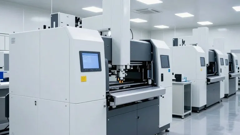
Export controls have blocked ASML from selling its most advanced extreme ultraviolet lithography machines to China. This restriction forces domestic chipmakers to rely on older deep ultraviolet equipment to manufacture critical components.
Industry experts tell Tom's Hardware that the workaround involves exposing critical chip layers multiple times. This method increases the risk of defects, extends production times, and raises the cost of each finished device. The financial burden grows with every additional exposure step required to print a single layer.
The gap between Chinese and Western capabilities remains substantial. Some analysts estimate the difference in access to EUV technology is five years or more. However, Chinese firms have achieved measurable progress using existing tools. A 2023 teardown of the Huawei Mate 60 Pro revealed that SMIC manufactured the Kirin 9000S processor using a second-generation 7nm-class process. Recent analysis suggests SMIC has since pushed its DUV-based process closer to 5nm density, though it still lags behind TSMC and Samsung.
The technical method is known as multiple patterning. Instead of printing a complex design in one pass, manufacturers break it into simpler patterns and build the layer incrementally. Chris Mack, co-founder and CTO of Fractilia, notes that three exposures on a 193 immersion tool cost roughly the same as one EUV exposure. At four masks, EUV becomes the more economical option for manufacturers.
Precision issues also affect profitability. Each new pattern must align perfectly with previous etching steps. More exposures lead to greater accumulated overlay errors. Designers often add extra space around features to compensate, which enlarges the chip size. This reduces the number of usable dies per wafer. Mack states that manufacturers sell die, not wafers, making the loss of yield a direct financial hit.
Data from the memory sector illustrates this efficiency gap. Morgan Stanley reported in June that CXMT produces only about one-third as many bits per wafer as Western rivals. The bank describes lithography access as a hard ceiling for Chinese memory development. Despite this, CXMT is planned to move to 1-alpha DRAM for HBM3e applications without using EUV. Morgan Stanley projects CXMT will increase its share of global DRAM bit supply from 14% in 2026 to 16% in 2028 by adding new capacity.
DUV technology still offers potential for advancement. Micron developed its 1-alpha DRAM without EUV, using tight process control to push 193 immersion limits. Mack describes this as the furthest any memory maker has pushed the technology. He believes China could achieve similar results if it leverages the full 193 immersion ecosystem, though he notes memory is easier to produce than logic chips.
The industry anticipates China will continue this trajectory. Morgan Stanley expects China's AI chip self-sufficiency to rise from 42% in 2025 to 70% by 2030. However, the bank maintains that EUV, high-bandwidth memory, and advanced software will remain areas where the West holds a distinct advantage.
Source: Tom's Hardware
More Business · Tech news · Business Watchdog · Report a business · Got a Story?